About Samsung Foundry
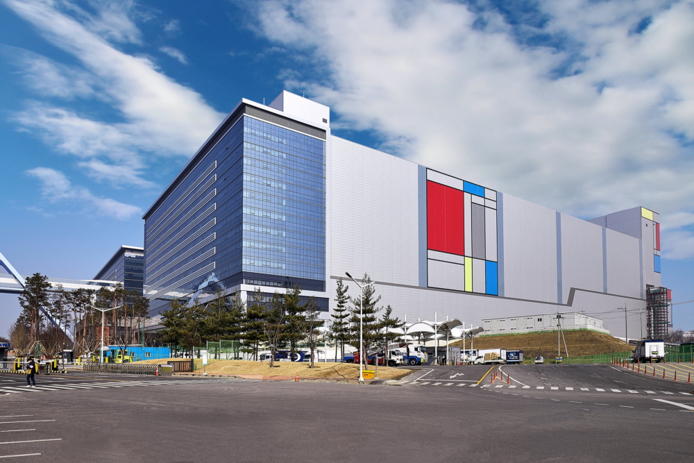
Samsung Foundry is the part of Samsung Semiconductor that makes chips other companies design. You bring a design, Samsung provides the process, the design kit, the IP libraries and the fab capacity, and ships wafers back. Samsung lists 28FD-SOI, FinFET nodes from 14nm through 4nm, 3nm gate-all-around with EUV, specialty processes for RF, embedded non-volatile memory, high voltage, BCD and image sensors, plus 2.5D and 3D advanced packaging and the SAFE design ecosystem of qualified EDA tools, IP and ASIC design services. It is the world's second largest foundry and has been for years. It is also, by revenue, a long way behind the first. Start from that fact rather than from a node name, because engaging a foundry is a multi-year commitment on yield, design kit maturity and capacity, and it is very expensive to reverse.
How big the gap to TSMC actually is
Second place in foundry is not a close second. TrendForce figures for the first quarter of 2026, as reported by TelecomLead, put total top ten foundry revenue at a record 47.95 billion US dollars. TSMC took 35.86 billion of that, a 72 percent share. Samsung Foundry took 3.2 billion, a 6.5 percent share, with revenue down 5.8 percent quarter on quarter on smartphone seasonality. That is roughly eleven times more revenue at TSMC than at Samsung in the same three months. Behind Samsung sat SMIC at 5.1 percent, UMC at 3.9 percent and GlobalFoundries at 3.3 percent.
Revenue share is a proxy, not a verdict on engineering, but it matters to a customer directly. Scale funds process development, it funds the IP and EDA ecosystem around a node, and it decides how much capacity exists when demand spikes. A foundry with 72 percent of industry revenue can bring several process variants to maturity at once. One with 6.5 percent has to choose.
Yields are the whole argument, and Samsung has been behind on them
A foundry sells finished, working die. What decides whether a node is worth buying is how many good die come off each wafer, because that sets your real cost per chip regardless of the wafer price you negotiated.
This is where Samsung's difficulty has been public. In April 2026 TrendForce, citing a Busan Ilbo report, put Samsung's 2nm yields in the mid-50 percent range, falling to around 40 percent once backend processing was counted, against a figure of roughly 60 percent generally treated as the threshold for comfortable mass production, and against reported TSMC yields of 60 to 70 percent. TrendForce had reported a similar 55 to 60 percent range in November 2025. These are second-hand industry reports rather than disclosures from Samsung, and yields move, but the direction has been consistent enough that customers have priced it in.
The roadmap tells a related story. Samsung originally targeted 1.4nm mass production for 2027 when it announced the node in 2022. That has moved to 2029, with SF1.4+ following in 2030. Meanwhile the SF2 family is being widened rather than superseded: SF2P, SF2P+ aimed at 2027 to 2028, then SF2X for AI and high performance work, and SF2Z with backside power delivery. High-NA EUV is not planned until the SF1A node around 2030. Tom's Hardware read the 1.4nm delay as Samsung slowing its leading edge cadence to make the SF2 family commercially competitive first, which is the optimistic reading and still an admission.
Who has signed, and who has walked away
The largest recent win is Tesla. In July 2025 Samsung and Tesla signed a foundry supply agreement worth 16.5 billion US dollars running to 2033, announced by Elon Musk and reported by CNN, Bloomberg and KED Global, covering Tesla's AI5 and AI6 chips at the Taylor, Texas fab. Reporting in July 2026 indicated AI5 volume is split between Samsung and TSMC while AI6 is allocated to Samsung's 2nm process at Taylor. Samsung has also been reported as a 2nm supplier for the Korean AI chip firm DeepX, targeting 2027.
The losses are as informative. TrendForce reported in April 2026 that Qualcomm had selected TSMC's N2P for its next flagship Snapdragon, having been expected to consider Samsung, and noted that Apple, Nvidia and AMD had not engaged Samsung for 2nm production. Qualcomm and Nvidia have both used Samsung nodes in the past. The highest volume, highest margin mobile and accelerator business has gone to TSMC.
So Samsung's leading edge customer list is short, concentrated and dependent on a few large agreements. That cuts both ways: you may get real attention, and you are exposed if the anchor customer changes plans.
What you are actually committing to when you pick a foundry
A foundry decision is not a price comparison. Once you tape out on a process you have bought that vendor's design kit version, its standard cell and IP libraries, its EDA tool qualifications, its packaging flow and its capacity queue. Porting a finished design to another foundry is close to redesigning it, and it costs a product cycle.
So the questions to ask are not on any node comparison chart. How mature is the process design kit, and how many revisions since first silicon? How many customers have taped out on this exact process variant, not just the family? What IP is already silicon-proven on it, and what would you fund yourself? What are the committed capacity terms, and what happens to your allocation in a shortage?
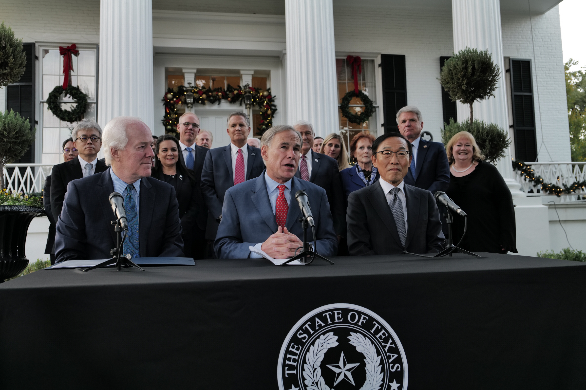
Samsung's genuine arguments are that it is the only credible alternative to TSMC at the leading edge, that it moved to gate-all-around earlier, and that a customer of meaningful size gets attention it would never get as a small account at TSMC. Its Taylor fab, announced in November 2021 as a 17 billion US dollar investment, gives US-based customers an onshore leading edge option that matters for defence, automotive and policy-sensitive work.
Who is better served by another foundry
Anyone who needs the highest performance leading edge silicon with the least schedule risk should be talking to TSMC first, and should be honest about why. The reported yield gap, the short customer list at 2nm and the 1.4nm slip are real, and a design whose whole value rests on being first to a node is the worst place to absorb them. The same goes for any product with a fixed launch window: a process still climbing its yield curve is a poor place to be, whoever runs it.
Anyone at mature nodes should look elsewhere entirely. If your design sits at 28nm and above, or on specialty analogue, power, RF or MEMS processes, the leading edge is irrelevant to you, and GlobalFoundries, UMC, Tower, Vanguard and X-FAB will usually offer better economics, longer node lifetimes and more attentive support.
Small volume customers should expect to work through a design service house or a multi-project wafer programme rather than approaching a leading edge foundry directly. Minimum commitments and mask set costs at these nodes rule out anything but high volume or very high value parts.
And anyone who arrived looking to buy Samsung memory, image sensors or Exynos processors is in the wrong place. Those are Samsung's own products. Foundry is the business of making somebody else's.
Reviews
No reviews yet
Nobody has reviewed Samsung Foundry here yet.